

n-GaN/p-GaN/u-GaN Wafer
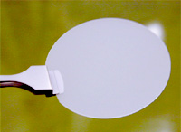 We are supplying n-GaN, p-GaN, u-GaN which are produced with epitaxial growth using our proprietary technology.
For your future request, we are offering other designed GaN.wafer, InGaN and AlGaN.
Please contact us to discuss wafer specifications in detail.

 SPECIFICATIONS
| Epi wafer diameter | 2 inch |
|---|---|
| Epi layer | GaN |
| Thickness of GaN epilayer | 2-10 |
| Structure of GaN epilayer | Wurtzite |
| Orientation of GaN layer | (0001) |
| Conductivity | N-type P-type undoped-type |
| Surface | as grown |
| Substrate | Sapphire |
| Substrate orientation | (0001) on-axis |
- *No buffer layer is required.
![]()